
Atomic Scale Design Network (ASDN)
Education and Research in Materials and Device Design
Atomic Scale Design Network (ASDN) is an internet gateway for a collaborative initiative of an international education and research community in
fundamental and applications oriented research, development and implementation of educational programs and development of new computational tools for academic and industrial applications.
We invite international scholars, researchers and educators, to join our solution center for the following tasks:
- ⚛ Organization of joint research projects;
- ⚛ Organization of regular international conferences and seminars;
- ⚛ Development of online educational programs;
- ⚛ Establishment of an international network of distributed computing resources
- ⚛ Development and commercialization of new software;
- ⚛ Development of applied research and partnership with industrial enterprises.
Tutorial pages at ASDN provide information about physics, chemistry and the biology of materials and their applications in technology and every day life while uncovering the roots of phenomena hidden in the atomic structure of matter. Browse our pages, learn, enjoy and come again!
ASDN Team
News and Updates
ASDN lecture on Quantum Chemistry Web Platform for Education - CalcUS Cloud Showcase by Raphael Robidas.
ASDN lecture on Turnover Frquncy of Heterogeneous Catalitic Reactions by Professor Dmitry Murzin.
ASDN lecture on Fuel Cell vs Battery Power by Professor Dominic Gervasio.
ASDN lecture on Computational Design of Biomaterials to address Viral Diseases by Matheus Ferraz.
ASDN webinar on Materials Revolution & Computational Gemology by Maryam, Mehya and Mubashir Mansoor.
We have introduced youtube channel Atomic Scale Design for Newbies, which is designated for undergraduate and K-12 students who want to try free atomic scale molecular and crystal design tools from curiosity or/and with a prospect to gain in-depth knowledge of atomic scale structure of materials.
Selected Tutorial Pages

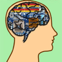
Brain Computer Interface
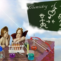
Chemistry of Love

Modern Architectural Acoustics
Silicates
Selected Links

Education
Energy

Funding
Software